2N2/6 Schematics
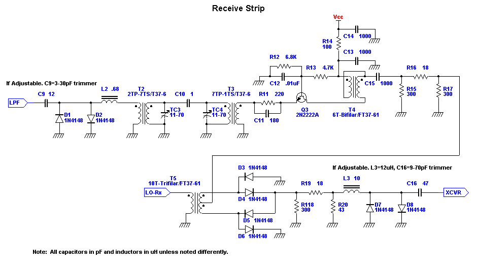
This is the schematic diagram of the receive strip. Note that in two locations, you can use an additional trimmer capacitor to replace a fixed capacitor. This change will enhance performance by a few dB, especially of the fixed inductors are off a bit due to normal tolerances. Transformer T5 is part of the single balanced receiver mixer, and is balanced for the LO signal, minimizing feedthrough of this component. The desired 7 MHz output signal is filtered by the series resonance of L3 and C16.
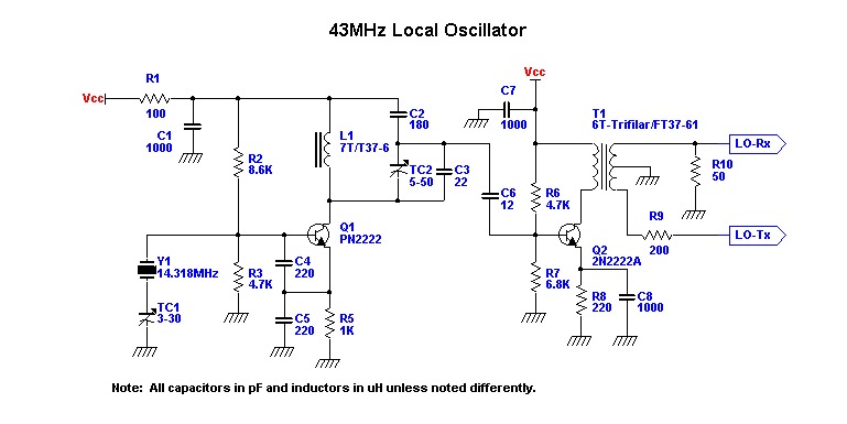
The schematic of the local oscillator section. TC1 is adjusted so that the crystal oscillates at 14 .333 MHz. TC2 is tuned for maximum 43 MHz signal output, the third harmonic of the crystal. Resistor R10 can be either 47 or 51 ohms. The LO-Rx signal level should be about +10 dBm, or 2 volts peak-to-peak.
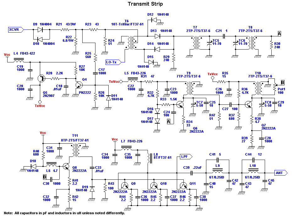
The transmit strip schematic is much more complex than the receive strip schematic, which was also apparent when comparing the respective block diagrams. Transmitted 7 MHz r.f. from the driving transceiver in passed through D9 and D10, which conduct with higher levels of r.f., but are essentially open circuits during receive. This signal is then attenuated to a level compatible with the single balanced mixer comprised of transformer T6 and diodes D12 through D15. Local oscillator signal is injected into the mixer at about +10 dBm. Like the receive mixer, this mixer is also balanced on the local oscillator signal, minimizing the amount of 43 MHz signal appearing at the output. The principle output signals are at 7 MHz, 36 MHz, and 50 MHz, i.e., the driving signal, and the local oscillator minus and plus the driving signal. These signals are passed to the coupled resonator filter comprised of T7/TC5 and T8/TC6, with the coupling being done by capacitor C21. This filter is tuned to 50 MHz, greatly attenuating all other signals. Transistor Q6 and Q7 are class A linear amplifiers with tuned outputs, and amplify the 50 MHz signal by 10 to 13 dB each, depending on the quality of the transistor used. During receive, this pair of amplifier have their supply voltage removed so that they don't generate noise, and obliterate the low level received signal. The supply voltage is switched on by rectifying some of the incoming drive signal, and using it to control transistor Q5. Further amplification occurs in transistor Q8, which is the untuned driver stage, and is operating class B, to conserve power during receive. The final amplifier consists of 3 parallel 2N2222A transistors running in class C. They can deliver a maximum of 2 watts of 50 MHz r.f. power if good transistors are used. The signal is then routed through an eliptic output filter with notches set for 100, and 150 MHz, the second and third harmonics. This filter helps assure compliance with FCC requirements for spectral purity. After filtering, the transmitted signal is sent to the antenna.
Back to the "2N2/6" page